Physical Design Course– SRIVIDYA VLSI
Physical Design Course
6 Months (Students, Freshers) Offline mode
5 Months (Working Professionals and Freshers) Online mode
- Exclusive Course Models For Freshers, Students, Professionals
- Designed and Delivered by Industry Experts
- RTL to GDS2 Flow Using Synopsys DC, ICC2, Prime Time Tools
- 14nm FINFET Libraries
- Mock Interviews With Industry Experts
- 100% Placement Support
- Projects: 2 block level
Master the Backbone of Chip Implementation with Industry-Focused Training
Are you ready to step into one of the most crucial domains of the semiconductor industry? SRIVIDYA VLSI’s Physical Design Course equips you with the real-world skills needed to turn RTL into GDSII – the final step before chip fabrication. Designed for engineering graduates, freshers, and working professionals, this course bridges the gap between academic knowledge and industry-ready expertise.
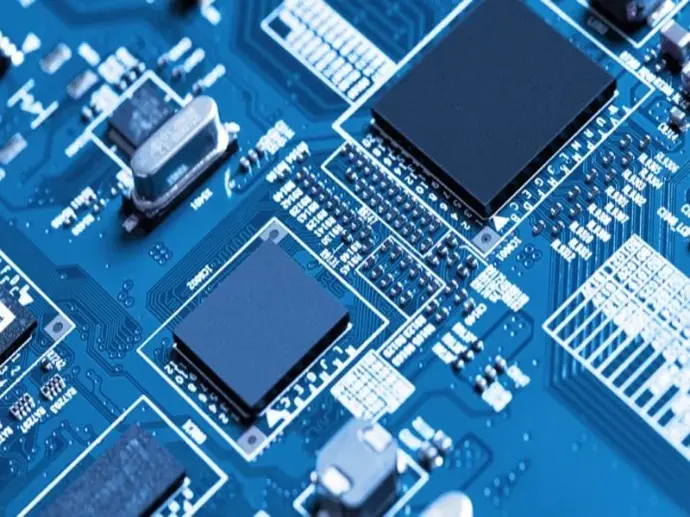
What is Physical Design?
Physical Design is a key phase in ASIC design flow where synthesized netlists are translated into physical layout. This includes floorplanning, placement, clock tree synthesis (CTS), routing, and design rule checks (DRC/LVS). It’s where the actual geometry of the chip is built – and timing, power, and area optimization are achieved.
At SRIVIDYA VLSI, we don’t just teach the flow – we help you understand the “why” behind every step using live project simulations and industry-grade EDA tools.
Why Choose SRIVIDYA VLSI?
- 📈 Industry-Relevant Curriculum:Designed in consultation with VLSI experts to meet the demands of the current chip design industry.
- 🖥️ Hands-on Training:Work on tools like Cadence Innovus, Synopsys ICC, or open-source equivalents to gain practical exposure.
- 👨🏫 Mentorship by Experts:Learn from seasoned professionals with years of experience in top semiconductor companies.
- 💼 Placement Assistance:Resume building, mock interviews, and direct placement opportunities through our hiring network.
- 🔁 Lifetime Access:Revisit recorded sessions and course material anytime.